WEEK 2
Week 2
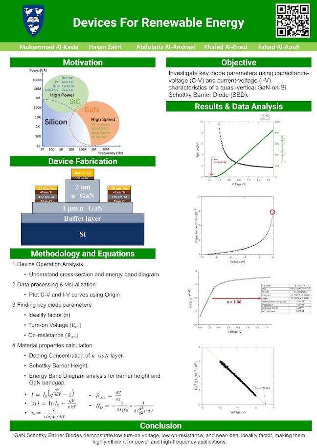
With our foundational data in place, we moved on to
extracting key electrical parameters. This was when things really started
getting interesting because we could see how different characteristics of the
diode were interrelated.
- The ideality factor (n) was found to be 1.08, indicating that the diode behaves close to the thermionic emission model with minimal interference from recombination or tunneling effects.

- The turn-on
voltage (Von) was determined to be 0.23V, which is much lower
than that of silicon Schottky diodes, making GaN a strong choice for
efficient power applications.

- The ON-resistance (Ron) was calculated at 1.8 ± 0.1 mΩ·cm², showing minimal conduction losses, a crucial feature for energy-efficient semiconductor devices.


These results highlighted the strong performance of
GaN-based diodes compared to silicon alternatives. It was rewarding to see that
our calculations made sense and aligned with published research.
Next Week's Task: We will determine the doping concentration of the n⁻ GaN drift layer and extract the Schottky barrier height using J-V characteristics. Two members will focus on doping concentration, while the rest will work on Schottky barrier height calculations. We also plan to discuss our findings with our supervisor to confirm we’re on the right track.


Comments
Post a Comment