Posts

Showing posts from February, 2025

Our Poster

Image

WEEK 5

Image
Week 5 February 28, 2025   This week was all about presenting our research! We finally got to share our findings with our peers and supervisors, and it was a rewarding experience. Each team member took turns explaining different parts of our project, making sure to highlight our key results and their significance. We received positive feedback and insightful questions that made us think even more critically about our work. One of the highlights of the day was taking a group picture with our supervisor to mark the completion of our project. It was a great way to celebrate the effort we had put in over the past five weeks.

WEEK 4

Image
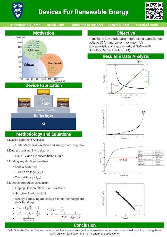
  Week 4 February 21, 2025  In our last week, we focused on refining our calculations and preparing for our final presentation. Seeing everything come together felt satisfying after weeks of effort. We calculated the effective density of states in the conduction band as 2.24 × 10¹⁸ cm ⁻ ³ , which matches theoretical expectations. We fine-tuned our Schottky barrier height calculation and arrived at 0.697 eV , confirming the efficiency of GaN SBDs for high-speed, low-power applications. Meanwhile, some of us worked on designing our poster to present our findings concisely. We aimed to make it visually engaging while clearly explaining our research. Balancing technical accuracy with simplicity for the audience was tricky, but we felt we struck the right balance by the end. The final few days were spent rehearsing our presentation and ensuring everyone was confident in explaining their sections. We were both excited and nervous, but overall, w...

WEEK 3

Image
Week 3 February 14, 2025  This week, we tackled two key calculations that required a deeper understanding of semiconductor physics. We had to revisit some fundamental concepts to ensure our approach was correct. Doping Concentration : By analyzing the 1/C² vs. voltage plot , we estimated a doping concentration of 1.601 × 10¹⁶ cm ⁻ ³ , which aligns well with values reported in existing literature. We were excited to see that our calculations made sense and matched theoretical expectations. Schottky Barrier Height : Using the thermionic emission model, we extracted the barrier height from the J-V characteristics, arriving at 0.611 eV —a crucial value affecting diode efficiency and leakage current. One challenge we faced was making sense of discrepancies between different approaches to extracting the Schottky barrier height. After some troubleshooting, we realized that minor variations in parameter assumptions could lead to different results, re...

WEEK 2

Image
Week 2 February 7, 2025  With our foundational data in place, we moved on to extracting key electrical parameters. This was when things really started getting interesting because we could see how different characteristics of the diode were interrelated. The ideality factor (n) was found to be 1.08 , indicating that the diode behaves close to the thermionic emission model with minimal interference from recombination or tunneling effects. The turn-on voltage (Von) was determined to be 0.23V , which is much lower than that of silicon Schottky diodes, making GaN a strong choice for efficient power applications. The ON-resistance (Ron) was calculated at 1.8 ± 0.1 mΩ·cm² , showing minimal conduction losses, a crucial feature for energy-efficient semiconductor devices. These results highlighted the strong performance of GaN-based diodes compared to silicon alternatives. It was rewarding to see that our calculations made sense and alig...